


pMosfetLevel0 - Level 0 Mosfet
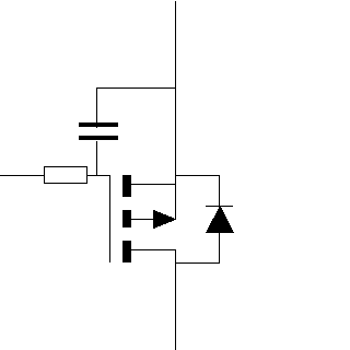
Connection Diagram:
| S | ||
| G |
| |
| D |
| Connections(3) | Position | Remark |
| S | Top | |
| G | Left | |
| D | Bottom |
| Parameters(6) | Default | Remark |
| VTO | -3 | Threshold voltage of the gate VGS_Threshold [volt] For p-type mosfets, enter a negative value |
| Cgs | 1nF | Mosfet Gate Source capacitance [F] |
| Rg | 10 | Mosfet internal gate resistance [ohm] |
| Rd | 10m | On state diode resistance [ohm] |
| Vd | 0.6 | On state diode voltage [volt] |
| Rds | 100m | On state mosfet RDS resistance [ohm] |
| Function | Ideal Mosfet model with inverse diode and gate delay | |
| Special | The Gate is a circuit node. The delay time due to charging CGS is modeled, | |
| Status | Standard | |
| Select from | Components\Library\Semiconductor\Mosfet | |
See also
MosfetDiode, MosfetLevel0, MosfetModule, MosfetModule4, MosfetMonitor, MosfetSensor, nMosfetLevel0, TrenchMosfetDiode, VDMOS,